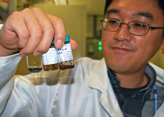
Hongshik Park Develops Carbon Nanotube Chip
Hongsik Park led an IBM research team in demonstrating the feasibility of linking large numbers of carbon nanotubes atop a silicon chip to create high-speed processors.
The breakthrough represents a big step toward commercializing carbon-nanotube-based processors that can outperform silicon-based chips by an order of magnitude.
The potential for carbon nanotubes to conduct digital computer signals five to 10 times the speed of conventional silicon chips has been postulated since carbon nanotubes were first discovered in the 1990s. The problem has been in getting the tubes — which are just few atoms in diameter — to string together in useful patterns because they tend to behave like spaghetti strands.
“It’s like trying to line up spaghetti, and doing it where the lines are just six nanometers apart,” said Supratik Guha, director of physical sciences at IBM Research and a spokesman for the team that did the work. “The thickness is just one nanometer.” A nanometer is a billionth of a meter.
By putting 10,000 of them in a useful grid pattern onto a silicon chip using mainstream manufacturing processes, Park and his team have taken carbon-nanotube chips out of the realm of the speculative and on track toward development of a radically more efficient microprocessor technology.
Aside from being much smaller than the smallest etchable dimensions of silicon chips, carbon nanotubes are inherently superior semiconductors because their electrons can move easier than those in silicon-based chips. That translates into potentially much faster, more energy-efficient processing of data.
The 10,000 nanotube transistors successfully arrayed by Park’s team is a far cry from the billions that will have to be arranged together to form chips superior to those in existence today. But it represents a quantum leap over prior efforts at arranging nanotubes which has been limited to just a few hundred nantubes.
“Carbon nanotubes, borne out of chemistry, have largely been laboratory curiosities as far as microelectronic applications are concerned,” explained Supratik Guha, Director of Physical Sciences at IBM Research. “We are attempting the first steps towards a technology by fabricating carbon nanotube transistors within a conventional wafer fabrication infrastructure. The motivation to work on carbon nanotube transistors is that at extremely small nanoscale dimensions, they outperform transistors made from any other material. However, there are challenges to address such as ultra high purity of the carbon nanotubes and deliberate placement at the nanoscale. We have been making significant strides in both.”
Carbon nanotubes are rolled from sheets of carbon just a single atom thick. At a functional thickness of less than 10 nanometers — about 10,000 times thinner than a strand of human hair and less than half the thickness of today’s cutting-edge silicon etching technology — they would enable processor-chip technology improvements of five to 10 times over current silicon chips.
Park’s team solved one of the biggest challenges of using carbon nanotubes — aligning them into perfectly regular patterns at high densities — by creating a new technique based on ion-exchange chemistry.
They began by mixing carbon nanotubes with a soapy surfactant to make them soluble in water. The carbon nanotube solution formed a bath into which was dipped a silicon substrate comprised of two oxides with trenches made of chemically-modified hafnium oxide (HfO2) and the rest of silicon oxide (SiO2). The carbon nanotubes attached via a chemical bond to the HfO2 regions while the rest of the surface remains clean.
Using this technique, Park’s team placed 10,000 carbon nanotubes on a single silicon chip at a density of about a billion per square centimeter.
What makes the IBM team’s work so promising is that it uses common chemicals and existing semiconductor fabrication equipment, making rapid further development of carbon nanotube semiconductors more practical.
Working with Hongsik Park were Ali Afzali, Shu-Jen Han, George Tulevski, Aaron Franklin, Jerry Tersoff, James Hannon and Wilfried Haensch.
Hongsik Park has been a research staff member at the IBM T. J. Watson Research Center, located in Yorktown Heights, NY, since July 2012. Before that he was a postdoctoral researcher at the Center since January of 2011.
Park completed his PhD work in electrical engineering at Brown University between 2006 and 2010. Before that he was a researcher in semiconductor device design and fabrication at the Samsung Advanced Institute of Technology between January 1999 and July 2006.
Park received a bachelors and masters in electrical engineering from Kyungpook National University in Daegu, Korea in 1998.

Hongsik Park led an IBM research team in demonstrating the feasibility of linking large numbers of carbon nanotubes atop a silicon chip to create high-speed processors.

