

The EUV Device that Enables Advanced Nvidia, Samsung and Intel Chips
By Goldsea Staff | 17 Nov, 2025
It took almost 40 years for ASML, a Dutch company once partly owned by Intel, TSMC and Samsung, to become the ultimate gatekeeper for cutting-edge AI and 5G chips.
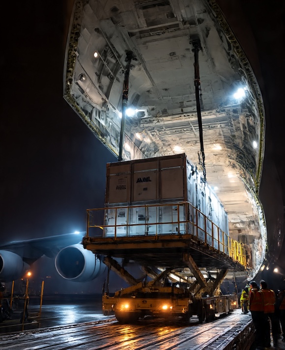
One portion of an ASML High-NA EUV lithography machine for chipmaking is loaded aboard a Boeing cargo plane. (Image by Meta)
Imagine a machine that produces 50,000 to 100,000 microscopic droplets of melted tin to be heated by a laser into plasma hotter than the surface of the sun in order to produce the extreme UV light (EUV) with a wavelength of 13.5 nm capable of sufficient resolution to etch 2 nm nodes onto silicon wafers.

An ASML EUV lithography machine in operation at a chipmaking cleanroom. (Image by Meta)
That degree of fine, precision etching is a critical step in producing chips of sufficient processing power and energy efficiency to play a role in the AI revolution.
Imagine a company whose importance to chipmaking was so great that Intel, TSMC and Samsung collectively took a 25.3% stake in 2012 to help ASML finance the development of EUV lithography to enable chips that are both more powerful and energy-efficient.
Now imagine a device whose four major modules must be assembled separately in the US, Germany and the Netherlands and costs about $400 million apiece, about as much as a Boeing 787 passenger jet. The modules of the ASML high-NA EUV lithography machines are so big and heavy that they require seven Boeing 747s or 25 trucks to transport them.

A greatly enlarged view of a microscopic droplet of molten tin being heated by a laser beam to turn it into a plasma that produces the 13.5 nm wavelength of extreme EV light needed for ASML's high-numerical aperture (High NA) EUV lithography for cutting-edge chipmaking. (Image by ChatGPT)
We tasked ChatGPT and Meta with providing answers to 2 questions that intrigued us about ASML:
1. The singularly essential role that ASML's EUV machine plays in modern technology made us wonder at the nature of the most crucial pieces of its technology.
2. We also wondered how a struggling joint venture launched in 1984 in a Philips backlot grew into the most indispensable technology company on earth.
The following compilations answer those 2 questions:
1. What makes ASML technology impossible for other companies to replicate?
Short answer: the EUV light source and the ultra-precision mirror/optical column — and ASML’s ability to integrate those pieces (plus metrology & control software) into a high-uptime system — are the single hardest things for rivals to copy. (ASML)
Why (concise breakdown):
Laser-produced plasma (LPP) EUV source — ASML (via Cymer) fires high-energy lasers at tin droplets to make a plasma that emits 13.5 nm EUV light. Generating that light reliably at the needed brightness and repetition rate (tens of kHz), while managing tin debris and system lifetime, requires mastery of plasma physics, high-power lasers, droplet delivery and debris mitigation that took decades to perfect. Rivals can reproduce pieces in labs but matching industrial throughput and uptime is extremely hard. (ASML)
Multilayer, ultra-smooth mirrors & optical column — EUV can’t use ordinary lenses; it uses many-layer Mo/Si mirrors with sub-angstrom surface precision and near-perfect cleanliness inside a vacuum. Making, aligning and protecting these mirrors (and the coatings that reflect EUV efficiently) is an exotic manufacturing capability—one slip in surface figure or contamination ruins performance. (ASML)
System integration, metrology and control software — Putting the fragile source and optics into a 100+-ton scanner that yields high wafer throughput requires massive systems-engineering: vibration isolation, thermal control, nanometer overlay, in-line metrology, and control software that continuously compensates tiny errors. That full stack — hardware + process know-how + supply-chain specialists — is what makes the machine usable in high-volume fabs. (ASML)
Other hard bits that reinforce the moat — EUV pellicles, mask making and mask defect control, and advancing to High-NA EUV (even tougher optics + alignment) are all technically brutal and protected by IP and long supplier relationships. (ASML)
Bottom line: competitors might copy individual technologies (a laser, a mirror stack) over many years, but reproducing the combined LPP source + multilayer optics + ultra-precise integration and production ecosystem at commercial scale is what makes ASML’s EUV systems uniquely hard to duplicate. (ASML)
ASML's High NA (High Numerical Aperture) EUV lithography machines are considered the most high-tech and unique aspect of their chipmaking equipment. These machines use extreme ultraviolet light with a wavelength of 13.5 nanometers to print incredibly small features on silicon wafers, enabling the production of more powerful and energy-efficient chips.Key Features of High NA EUV Machines:- Higher Resolution: The High NA system allows for the creation of smaller, more precise patterns on silicon wafers, improving chip performance and reducing production time.
- Increased Yield: High NA machines enable chipmakers to fit more transistors onto a single wafer, resulting in faster and more efficient chips.
- Improved Efficiency: ASML's High NA technology reduces the need for multiple mask exposures, improving throughput and cost-efficiency.
- Advanced Mirror Technology: The machines use ultra-precise mirrors crafted by German optics company Zeiss, which are considered the flattest surfaces in the world.
- Complex Logistics: Each High NA machine consists of four modules built across the US, Germany, and the Netherlands, requiring seven Boeing 747s or 25 trucks for transportation .
These machines are truly cutting-edge, with a price tag of around $400 million each, and only five units shipped so far, with Intel, TSMC, and Samsung being the early adopters .
2. How did ASML build itself from startup into the world's most valuable manufacturing hardware company?
In the summer of 1984, two companies—Philips, the Dutch electronics giant, and ASMI, a scrappy semiconductor-equipment maker founded by Arthur del Prado—quietly carved out space in a nondescript building in Veldhoven. They called their joint venture ASM Lithography. No one imagined it would one day hold the keys to the world’s most complex machines, or that entire national economies would orient their semiconductor ambitions around it.
At the time, ASML was an underfunded long shot. The company was born into a world dominated by Japanese and American lithography firms, with Nikon and Canon controlling the high ground and U.S. competitors fiercely guarding their market share. The fledgling Dutch team needed a breakthrough; what they had instead was a first-generation “stepper” machine that barely worked and a balance sheet that terrified anyone who saw it.
Yet ASML possessed one decisive advantage: it had nothing to lose. While industry giants optimized existing technologies, ASML took unpopular bets—modular designs, new wavelengths, riskier physics—and doubled down on partnership rather than secrecy. This openness would become the company’s signature strategy.
The PAS 5500 and ASML’s First Rise
The turning point arrived in the early 1990s. ASML released the PAS 5500, a deeply modular deep-ultraviolet (DUV) system that could be upgraded in pieces rather than replaced wholesale. It was a simple idea that solved a complex problem: chipmakers needed flexibility as nodes shrank and process windows tightened. The 5500 became a workhorse of the industry. For the first time, ASML had a platform—both technological and financial—from which to grow.
With the company’s IPO in 1995, ASML finally had capital to chase bigger ambitions. Those ambitions would soon collide with one of the most formidable challenges in modern engineering: extreme ultraviolet lithography (EUV).
The Two-Decade Gamble on EUV
By the late 1990s, it was clear that pushing DUV deeper into the nanometer regime would require increasingly tortured optical tricks. EUV, with its 13.5 nm wavelength, promised a cleaner path, but almost no one believed it could be made practical. The light was too weak, the materials too fragile, the optics too exotic.
ASML disagreed. It began pumping hundreds of millions into EUV research—at first through public-private partnerships, then through direct investment in its own ecosystem. In 2012, ASML made its most consequential purchase: Cymer, the American company developing a laser-produced plasma (LPP) light source by firing high-energy pulses at tin droplets. This was widely considered the “impossible” part of EUV. ASML decided it had to own it.
That same year, ASML pulled off a strategic masterstroke. Intel, TSMC, and Samsung—the titans of global chipmaking—each bought minority stakes in the company, collectively investing billions to accelerate EUV development. Never before had ASML’s customers invested directly in its R&D. It was a signal to the world that the most advanced players were betting the future of logic and memory on EUV—and on ASML.
The Zeiss Partnership: A Hidden Core
If Cymer provided the heart of EUV, Carl Zeiss SMT provided its nervous system. EUV could not use lenses; it required multilayer mirrors with atom-level surface precision. ASML and Zeiss built an R&D partnership so tight that the two organizations effectively functioned as one company for optical design.
Each mirror required more than 100 alternating layers of molybdenum and silicon, deposited with sub-angstrom uniformity, polished to a fraction of a wavelength, and kept in pristine vacuum to avoid contamination. The engineering was harder than building a space telescope. In fact, some EUV optics exceed the precision of NASA observatory mirrors.
The Breakthrough
After two decades of skepticism, budget overruns, and endless delays, the impossible happened. In 2019, ASML’s EUV scanners finally entered high-volume manufacturing. TSMC used them to build Apple’s 5-nanometer chips, and the smartphone in nearly every pocket suddenly relied on the output of a single Dutch company.
By 2023, EUV was no longer speculative—it was the backbone of advanced semiconductor production. ASML had become not merely a supplier, but the strategic choke point for every country or company aspiring to lead in AI, 5G, high-performance computing, or military-grade electronics.
High-NA and the New Frontier
Never content to rest, ASML pushed further. Its High-NA EUV systems, shipping to Intel and others beginning in 2024, reduce feature sizes another 70% and introduce geometries essential for 2-nanometer and post-2-nanometer nodes. Each system is the size of a bus, weighs over 100 tons, contains thousands of subsystems, and costs more than a Boeing 787.
And every one of them depends on the unlikely alliance of ASML, Cymer, Zeiss, TRUMPF, AGC, Hoya, and hundreds of ultra-specialized suppliers that grew around ASML like a self-reinforcing technology ecosystem.
From Underdog to Gatekeeper
ASML’s ascent was not inevitable. It was the product of long bets, stubborn engineering, and partnerships that required extraordinary trust. In an industry where secrecy once ruled, ASML became the company that collaborated its way to a monopoly.
Today, it is the sole producer of EUV lithography machines—devices so complex that no nation, no matter how wealthy, can replicate them alone. The world’s most advanced chips flow through ASML’s tools, and in a sense, so does the future of digital civilization.
From a patched-together workshop in Veldhoven to the center of the global tech ecosystem, ASML’s story is not just a tale of technological triumph. It is a story of how vision, persistence, and improbable alliances can reshape the trajectory of an entire industry.
Recent Articles
- SpaceX IPO Already Two Times Oversubscribed
- SpaceX Signs Google As AI Compute Client After Landing Anthropic
- $1 Trillion in Stock Market Valuation Eraced by AI Chip Selloff
- Anthropic Urges Industry Pause As AI Nears Recursive Self-Development
- Trump's South Lawn UFC Birthday Bash to Mix Politics with Punches
- Trump Policies Targeting 39 Nationalities of Immigrants Invalidated
- Ryan Tseng's $13 Billion Shield AI Flies High Despite V-BAT Crashes and Severed Fingers
- India's Q1 GDP Growth Robust as Domestic Demand Offsets Iran Impact
- China and Hong Kong Users Blocked from SpaceX Website, IPO Documents
- SpaceX Revenue to Hit $3.4 Trillion in 2040 on AI Demand, Projects Morgan Stanley